mip-T113

Features

  • Adjustable voltage/current reference

  • Processor or sensor supply possible

  • Two Current and one voltage output stages

  • Controllable current sources with internal driver stages

  • Voltage output short circuit / reverse polarity protection

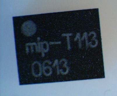
  • Small package: QFN18 (5mm x 4mm x 0.9mm)

Operating area

  • Temperature range: -40 – 105°C

  • Voltage range: VCC = 2.5 – 28V

  • Current output: IIo ≤ 20mA intern

  • Regulator current: IVCR ≤ 25mA

Applications

  • Sensors, voltage/current converter

  • Controllable current and voltage sources
  • 0 – 5/10V, 0/4 – 20mA-Interface

  • Automation, Building, Medicine, ...


Description
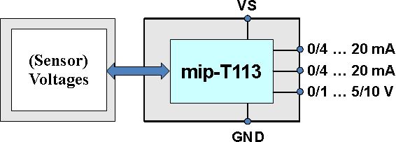
The mip-T113 was developed for the standard 0/4 – 20mA-current- (twice) and voltage (protected) interfaces. The circuit is also suitable as LED driver (brightness control possible) or as controllable current and voltage source.The 20mA current of the interface can driven directly by the circuit, with additional external npn transistors currents up to 2A are allowed. Also the circuit contains an adjustable voltage/current regulator, which can supply and protect the remaining components (sensor, processor, …).

Block diagram
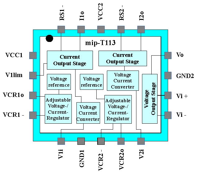

Typical Application